

CUHK
News Centre
CUHK achieves breakthrough techniques taking nanoscale 3D printing into a new era
Multi-material 3D fabrication at nanoscale has been the holy grail of nanotechnology and a key enabler for the development of new technologies, including photonic, electronic, and biomedical devices. Professor Chen Shih-Chi and his team from The Chinese University of Hong Kong (CUHK)’s Department of Mechanical and Automation Engineering, in collaboration with Professor Zhao Yongxin from Carnegie Mellon University (CMU)’s Department of Biological Sciences and Professor Zhao Ni from CUHK’s Department of Electronic Engineering, have developed a 3D nanofabrication platform that for the first time realises multi-material fabrication, meaning it is able to make a great variety of materials, including metals, alloys, semiconductors, polymers, ceramics and biomaterials at a record-setting resolution of 20 nanometers, and a light patterning speed of 300 mm3/hour, three orders of magnitude faster than conventional serial fabrication systems that are currently used in the commercial world. The achievement has recently been published in the journal Science, affirming its status as a technological breakthrough that leads nanoscale 3D printing into a new era.
Everything started three years ago, when Professor Chen visited CMU as an invited speaker. An inspiring conversation he had with Professor Zhao at CMU sparked a collaboration between the two researchers, aiming to find new solutions to long-standing challenges in nano- and micro-fabrication: developing ways to break the limit on material selection and improve the resolution of printable nanodevices to as small as 10 nanometres at a reasonable fabrication rate for practical applications.
Professor Chen is known for inventing the femtosecond projection two-photon lithography system (an ultrafast nano-printing method, reported in the journal Science in 2019), while Professor Zhao’s Biophotonics Lab develops novel techniques to study biological and pathological processes in cells and tissues. They decided to combine their techniques and expertise to pursue the radical idea. The results of their collaboration have opened new doors for the realisation of sophisticated nanodevices.
“A major challenge in nanotechnology is to fabricate complex 3D structures with materials beyond polymers and noble metals, which was previously limited by photo-initiated chemical reactions. Based on the unique surface properties and nano-structures of the femtosecond light sheet-patterned hydrogel found by our team, we proposed a kinetically controlled nano-assembly process to substitute the conventional photo-reactions. As the strategy mainly relies on the physical properties of functional materials, such as sizes or hydrophilicity, the limit of material selections can be entirely overcome. Next, by shrinking the patterned gel substrate in acid, we can easily break the diffraction barrier,” said Professor Chen.
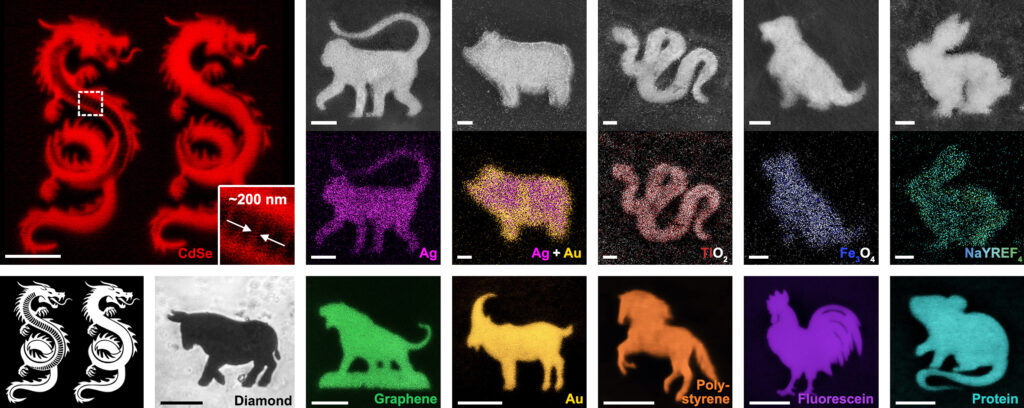
As a result, the team developed a general strategy for fabricating arbitrary 3D nanostructures with a library of materials including metals, metal alloys, 2D materials, oxides, diamond, upconversion materials, semiconductors, polymers, biomaterials, molecular crystals and inks. In their research, hydrogels patterned by femtosecond light sheets were used as templates that allow for direct assembly of materials to form designed nanostructures. By fine-tuning the exposure strategy, the features of the patterned gel and the kinetic effects, the team realised 2D and 3D structures of 20- to 200-nm resolution.
To demonstrate the promising capabilities of the new method, they fabricated nanodevices, including encrypted optical storage, diffractive optical elements and microelectrodes, to showcase the precision and the designed functions. The optical storage device set a new record for storage density (1.14 petabit/cm3, approximately three orders of magnitude higher than the previous record), and simultaneously set a new record for data-writing speed (84 Mbit/s), owing to the high-speed nature of the femtosecond projection method. These results showed that the method provides a systematic solution for nanofabrication across different classes of materials, and opens up further possibilities for the design of sophisticated nanodevices, creating pathways for viable manufacturing of a whole range of technologies.
Professor Chen further explained, “The true importance of this work lies in the fact that the method simultaneously achieved all key metrics in manufacturing: resolution, fabrication rate and cost. This means our new method can not only be used to make micro- and nanodevices not previously possible, but can make them at high throughput and low cost for practical applications in photonics, health, automobiles and even aerospace.”
In the future, the researchers’ goal is to build functional nanodevices with multiple materials, like nanocircuits, nanobiosensors, light-emitting diodes, and lasers, for different applications.
Other authors of this work include Han Fei and Gu Songyun (co-first authors) from CUHK, and Klimas Aleks from CMU. The full text can be found at https://www.science.org/doi/10.1126/science.abm8420.


video:
Demonstration of the femtosecond light sheet patterning process (i.e. “CUHK”) and the following self-assembly of fountain pen ink (under an optical microscope).
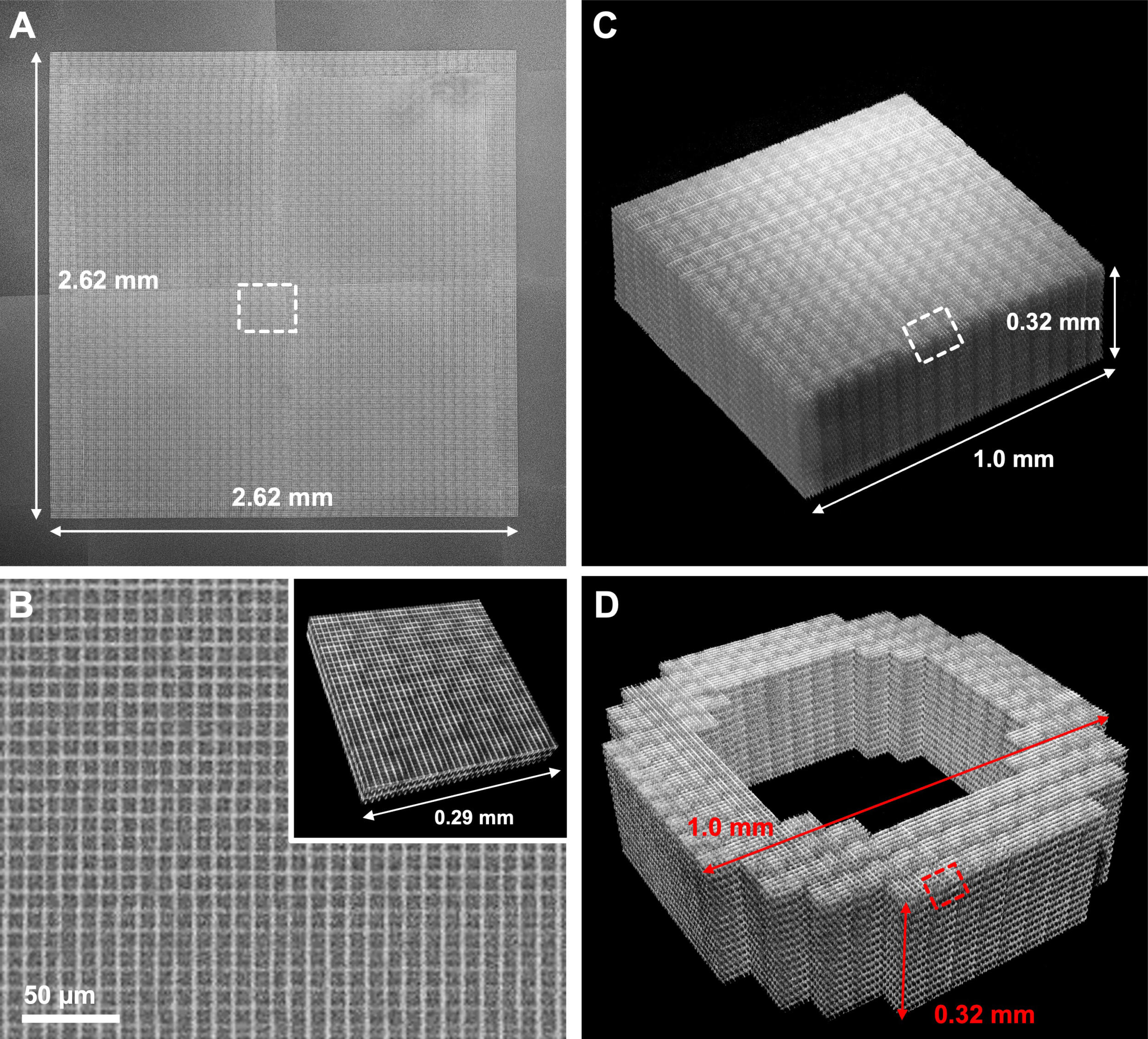
Fabrication of large-scale woodpile structures: (A) 12-layer woodpile structure of florescent polystyrene (top view, stitched from 16 sub-images due to the limited microscope field of view); (B) zoomed-in view of (A), where the inset shows a 3D fluorescent image of the structural details in the selected area; (C) cuboid woodpile structure of florescent protein; (D) O-shaped 3D woodpile structure of CdSe.

Demonstration of material variety via 12 Chinese zodiac animals, including fluorescent image of two dragons of CdSe quantum dots (QDs) without shrinking (the inset shows a resolution of ~200 nm); SEM (top) and EDX (bottom) images of a monkey of Ag; pig of Au-Ag alloy; snake of TiO2; dog of Fe3O4; rabbit of NaYREF4; optical microscopy image of an ox of diamond; fluorescent images of a tiger of graphene QDs; goat of fluorescent Au; horse of polystyrene; rooster of fluorescein; and mouse of fluorescent protein.
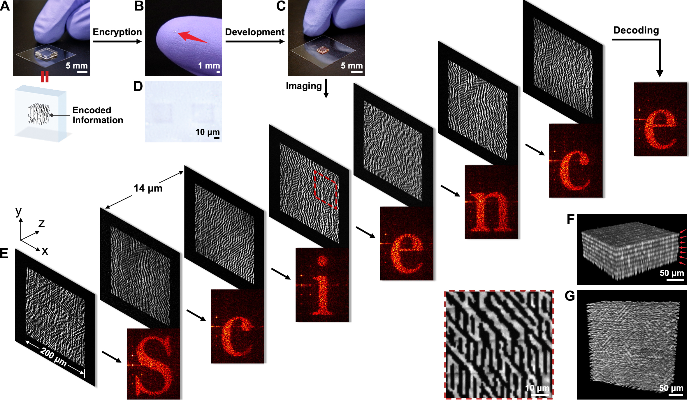
Demonstration of optical storage and encryption: (A) an expanded hydrogel patterned with designed information; (B) the gel in (A) after fully shrinking and dehydration to realise physical encryption; (C) the re-expanded gel is deposited with CdSe and developed to decrypt the stored patterns; (D) Optical image showing two encrypted seven-layer hologram patterns in (B); (E) Fluorescent images of the decrypted holograms, decoding the word “Science”; and (F, G) 3D views of the decrypted holograms.
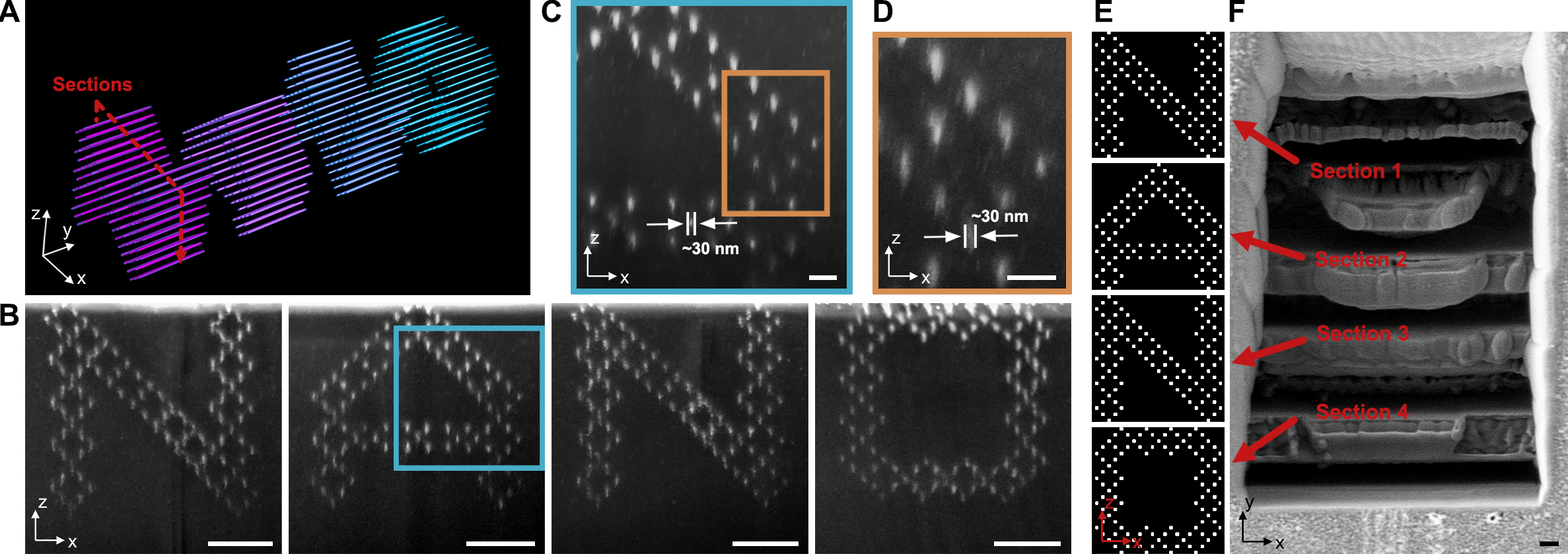
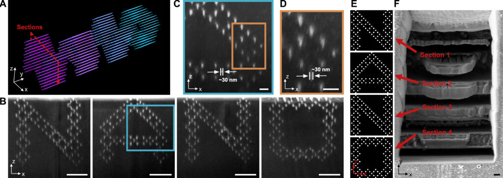
Nanostructures demonstrating minimum feature sizes. (A) 3D model of a nonconnected “NANO” structure comprised of arrays of parallel nanowires; (B) SEM cross-sectional images of the “NANO” structure cut by a focused ion beam (FIB); (C) zoomed-in view of the letter “A” in (B); and (D) zoomed-in view of (C); (E) Four cross-sectional patterns of the “NANO” structure (in the x-z plane of (A)); (F) SEM images showing the trenches of the gel sample opened by an FIB-cut, where the positions of each letter are labelled. All cross-sectional images were taken at a substrate tilt angle of 52°.